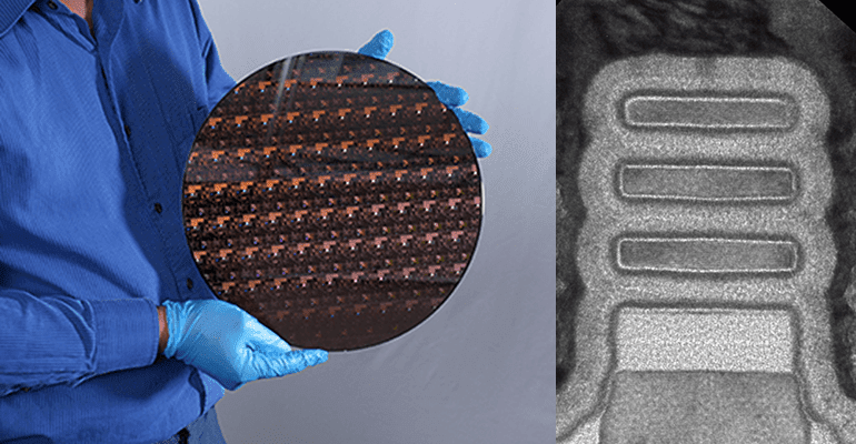
IBM has recently announced that it has created the world's first 2nm node chip.
2nm is possible!
AnandTech explained that while it is called the 2-nanometer process node, it doesn't have an equivalent metric for the 2D structure size of the chip. This is due to the 3D transistor design making it equivalent to a 2D transistor design.
IBM explained that versus the modern 7nm processors, its 2nm process will improve the performance by 45 percent and 75 percent less energy.
It added that the tech can fit 50 billion transistors onto a chip the size of a fingernail. IBM's definition of a fingernail is 150 square millimeters. This means that it has a transistor density of 333 million transistors per square millimeter (MTr/mm2).
In comparison, Taiwan's TSMC has around 171 million transistors per square millimeter.
IBM added that a 2nm chip will "quadruple" battery life on smartphones which can give around 4 days of juice on a single charge.
This will also reduce the carbon footprint of data centers as it reduces the number of chips required to run services, laptops will be faster, and provide object detection in autonomous cars.
They will also reduce the carbon footprint of data centers, by reducing the number of chips required to run servers. In addition, laptops will become faster as will object detection in autonomous cars.
More transistors on a chip also means processor designers have more options to infuse core-level innovations to improve capabilities for leading-edge workloads such as AI and cloud computing, as well as new pathways for hardware-enforced security and encryption
IBM's new 2nm chip design is a proof of concept for now which means that we won't see this tech on consumer products anytime soon.
IBM Research is also exploring options for continued scaling to 1nm and beyond.
Expect to see 4nm late this year and 3nm chips in the second half of next year first.


